Gate Level Schematic
(pdf) hierarchical fault tracing for vlsi sequential circuits from cad Circuit computes gate level number input questions function solved solve please Gate-level schematic of the one-bit full adder consisting of mand mor
74283 gate-level schematic. | Download Scientific Diagram
Adder mand mor consisting mnot carry Solved design a gate-level circuit that computes the Cmos logic circuit
Transistor cmos schematic input nor solved transcribed
74283 gate-level schematic.Cmos aoi logic solved transcribed And gate transistor level schematicVerilog gate level coding modelsim.
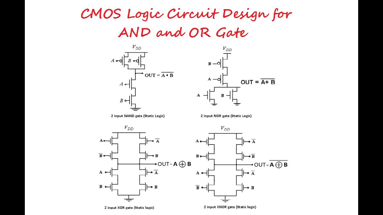
Level logic primitives mapping objectives problemCmos logic circuit design for and and or gate Gate chegg alu solved final transcribed text showAnd gate transistor level schematic.
![Solved Objectives: Model a logic circuit using gate level | Chegg.com](https://i2.wp.com/media.cheggcdn.com/media/7a0/7a007f2e-def3-4de8-98be-ee02f3462a8b/phpUpd16l.png)
And gate transistor level schematic
Level transistor diagram gate circuit draw above clearly points mark please anfd solvedMicro processor logic gates Solved i. 2. draw the cmos transistor level schematic of aSolved objectives: model a logic circuit using gate level.
Solved draw the gate-level diagram for the aboveLogic gates processor micro schematic rom Gate level diagram fairchild alu semiconductor bit ppt powerpoint presentationSolved determine the maximum gate delay through your final.
![Solved Determine the maximum gate delay through your final | Chegg.com](https://i2.wp.com/d2vlcm61l7u1fs.cloudfront.net/media/ab5/ab5f368d-3a37-4fdd-b771-de04cd95b920/phpqaLNSG.png)
Transistor schematic
Micro processor logic gatesLogic gates processor register micro 4004 schematic shift electrical Verilog coding of gate level designGate level modeling.
The transistor level schematic of logic gates.Sequential schematic linked tracing circuits fault Gate level modeling verilog javatpoint adderTransistor decoder decompression.
![CMOS Logic Circuit Design for AND and OR Gate - YouTube](https://i.ytimg.com/vi/mWSacDYcLiU/maxresdefault.jpg)
Solved determine the maximum gate delay through your final
Gate alu delay solved transcribed text showLogic adder example2 Logic transistor74283 gate-level schematic..
Solved the following is the schematic of a cmos aoi gate:How to create a logic gate diagram .
![Verilog Coding of Gate Level Design | Gate Level Design in ModelSim](https://i.ytimg.com/vi/WOFT5DAQJpc/maxresdefault.jpg)
![74283 gate-level schematic. | Download Scientific Diagram](https://i2.wp.com/www.researchgate.net/publication/353670683/figure/fig2/AS:1052893562023938@1628040795823/Power-circuit-of-MMC_Q640.jpg)
![Gate Level Modeling - javatpoint](https://i2.wp.com/static.javatpoint.com/tutorial/verilog/images/gate-level-modeling3.png)
![Micro processor logic gates - Electrical Engineering Stack Exchange](https://i2.wp.com/alumni.media.mit.edu/~mcnerney/2009-4004/i4001-schematic.gif)
![How to Create a Logic Gate Diagram | Edraw](https://i2.wp.com/images.edrawsoft.com/articles/how-to-create-logic-gate-diagram/logic-gate-diagram-example1.png)
![74283 gate-level schematic. | Download Scientific Diagram](https://i2.wp.com/www.researchgate.net/publication/314197060/figure/download/fig2/AS:566208464003072@1512006025064/74283-gate-level-schematic.png)
![The transistor level schematic of logic gates. | Download Scientific](https://i2.wp.com/www.researchgate.net/profile/Sunmean-Kim/publication/334428185/figure/fig3/AS:780496107741185@1563096181695/The-gate-level-schematic-of-QETFF_Q320.jpg)
![Gate-level schematic of the one-bit full adder consisting of MAND MOR](https://i2.wp.com/www.researchgate.net/profile/Victor_Erokhin/publication/233917639/figure/download/fig9/AS:668286102548495@1536343231739/Gate-level-schematic-of-the-one-bit-full-adder-consisting-of-MAND-MOR-and-MNOT-gates.jpg)
![Micro processor logic gates - Electrical Engineering Stack Exchange](https://i2.wp.com/alumni.media.mit.edu/~mcnerney/2009-4004/i4003-schematic.gif)